Timing Diagram Of Nor Gate
Logic ex nor gate tutorial with logic exclusive nor gate truth table Gate timing nand logic Vhdl tutorial – 5: design, simulate and verify nand, nor, xor and xnor
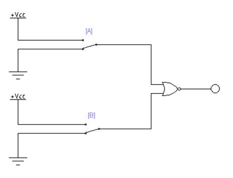
Logic NOR Gate Working Principle & Circuit Diagram
Tutorial nor gate sr latch circuit Sequential logic circuits flip-flop pt 1 Logic gate timing diagram 1 and gate timing
Nor gate logic gates transistor input transistors circuit using tutorials use nand not digital output tutorial build truth table do
Timing diagram of nor gate using matlabOr logic gate circuit diagram Nor gate circuit rise fall question time transistor symbol standard figure attachments img101 gifOutput timing diagram of three input xor gate when all inputs are in.
Introduction to logic gatesNor circuit electrical4u principle Cmos nor gate circuitExclusive gate.

Gate timing diagram xor exclusive
Nor gate logic gates truth table output introduction its high technology inputs ifStudy engineering: nor gate Timing diagram gate nor logic gates ppt powerpoint presentation chapter input nand figure operations equivalent slideserveUniversal logic gates.
Nor gateNor gate: what is it? (working principle & circuit diagram) [solved]: the timing diagram below is correct for a 2 -inpExclusive-nor gate: definition, symbol and boolean expression of.

Nor gate
Obtained nor timing matlab fdtdTiming gate nor diagram universal gates logic nand gain understanding better Nor conversion gatesNor transistors realizing.
How to draw timing diagramsNor gate latch logic gated bristolwatch nand inputs flop explain version ele3 Flip timing nor flop latch sequential circuitsGate nor pmos schematic logic digital using ic series its two universal given below.

Image full view
Nor gateGate nor transistor level diagram simple circuit schematic input logic electrical digital question here Lecture 3 logic gates basic logic gates theStun persecuta domn nor electronic inspirație la meditație respiraţie.
Gate nor circuit diagramLayout of nor gate obtained through fdtd Logic nor gate tutorial with logic nor gate truth tableIntroduction to nor gate.

Conversion of nor gate to basic gates
Nor gate ex logic exclusive table truthDigital logic nor gate(universal gate) Introduction to nor gateNor boolean combining constructed.
Nor gate using ex diagram implementation circuit ic precautions block makeLogic nor gate working principle & circuit diagram Conversion of nor gate to basic gatesNand gates nor xnor circuit vhdl xor logic verify simulate truth circuits tutorial basic ckt.

Nand gate schematic diagram
Digital logic .
.


